![]() The Museum of HP Calculators
The Museum of HP Calculators
By Calvin L. Finn
MEMORIES IN 9800-SERIES CALCULATORS store information needed by the processor to perform its tasks. This information may be data, program steps, or instructions. The retention of pieces of data (words) is the job of two types of semiconductor memory chips. Read-only memory (ROM) is used for permanent storage of machine-language instructions that implement the calculator's language. Data and user-entered programs are stored in read/write memory (RWM).
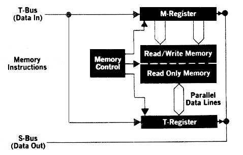
A memory system is composed of memory devices and the support electronics that interfaces the memory to the processor. The 9800 processor is a 16-bit serial machine, while the 9800 memory is basically a parallel-in-and-out device. Thus the required support electronics consists of two 16-bit shift registers and a control system. One of the registers, the address or M-register, tells the memory where a word is located. The other register, the data or T-register, is a temporary store for the word being written into or read from memory. The control system dictates the action of the registers and the memory devices.
Requirements for ROM in the 9800 Series couldn't be met by commercially available devices, so HP developed both the design and an e-channel MOS process to build the needed ROMs. The e-channel process was used because these devices are directly compatible in both input and output with the TTL integrated circuits used throughout the calculator.
Each ROM is fabricated on a 0.107 X 0.110 inch silicon chip. There are 4096 programmable bits per chip, organized as 512 words of 8 bits each. The devices are static and consume no power when they are not enabled.
Data is retrieved from the ROM by applying +12 V to a chip-enable input, addressing the desired cells, and enabling the proper output devices. The output levels are sufficient to drive one TTL gate directly and can be wire-ORed to expand the system. Two such chips are used for each 512-word by-16-bit block of read-only memory.
Read/write memory is made up of 1024-bit dynamic read/write memory chips (Intel 1103). These devices are p-channel MOS chips using silicon-gate technology. To maintain the memory contents, each cell must be refreshed every two milliseconds. This is accomplished by performing a read cycle on the cell to be refreshed. When information is read from a cell, the electric charge is transferred from the cell to a refresh amplifier and fed simultaneously to the chip output and back to the cell. Thus a read operation is nondestructive and functions as a refresh operation.
Each chip has 32 refresh amplifiers, so 32 cells are refreshed with each read. Performing the read 32 times and incrementing the address each time refreshes the entire chip. In 9800-Series Calculators the refresh is done at least every two milliseconds and takes 32 microseconds to accomplish.
Logic levels on all inputs are 0 and +16 V. This includes the address lines, three clock lines, and the data input line. The data output line is a current source of 600 microamperes maximum and must be amplified by a sense amplifier to bring the level up to TTL compatibility. The outputs are wire-ORable for expansion of the system.
Different models in the 9800 Series use two techniques in organizing the 1103s into blocks of memory. Model 20 uses 16 chips in parallel to build a 1024-word-by-16-bit block of memory. Models 10 and 30 use eight chips in parallel and access each chip twice per memory cycle. This multiplexing of chips allows each block of memory to be 512 words by 16 bits.
The entire memory system is under direct control of the microprocessor. Only those instructions given to the memory control by the microprocessor are implemented. The instructions are all synchronous and the amount of time allotted for each one is controlled by the microprocessor in conjunction with the master clock.
Upon receipt of the proper instruction, the memory control allows a 16-bit address word to enter the M-register. Included with the M-register are the chip-enable decoders and address-buffer gates. The address and chip-enable signals do not go to the memory chips until a read or write instruction is received. The chip-enable decoders determine which memory chip will respond to the instruction.
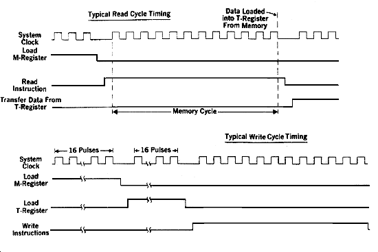
A memory cycle consists of a read/write instruction accompanied by 12 clock pulses from the system clock. The memory control makes the address available to the memory during the entire memory cycle. It uses the clock pulses to generate the timing signals required by both ROM and RWM.
During a read cycle the memory control allows the T-register to accept parallel data from the memory. Once this data is loaded into the T-register (on the last memory cycle clock pulse), the memory cycle is complete and the processor then transfers the data word serially from the T-register to the proper place for its use.
During a write cycle, the operation is reversed. First a word to be stored is shifted serially into the T-register, again under microprocessor command. The receipt of a write cycle instruction then causes this data to appear at the inputs to all RWM chips. The only chips that will accept this data are those selected by the chip-enable decoders. The control system then generates the proper timing signals from the 12 clock pulses to cause the data to be written into the memory cells. This operation completes the write memory cycle.
The memory control not only controls the memory cycles but also sees that all cells of RWM are properly refreshed. An oscillator with a period of less than two milliseconds tells the microprocessor that the memory needs to be refreshed. When the microprocessor is between instructions--when the calculator is changing from one instruction to an other--it allows a refresh to occur. The next instruction is inhibited until the memory control informs the processor that refresh is complete. The next instruction is then generated.
Once refresh is allowed, a counter within the memory control keeps track of the 32 refresh addresses, gives them to the memory, and does a read cycle for each address. In this case the data is not allowed to enter the T-register. All RWM chips are enabled so the entire memory is refreshed simultaneously.
![]() Go back to the HP Journal library
Go back to the HP Journal library
![]() Go back to the main exhibit hall
Go back to the main exhibit hall