![]() The Museum of HP Calculators
The Museum of HP Calculators
by Norman L. Johnson and Vijay V. Marathe
COMPLEMENTARY METAL-OXIDE semiconductor (CMOS) technology plays an important role in many recent HP products. Most of these products use the silicon-on-sapphire (SOS) form of this integrated circuit technology. However, there is another form: bulk CMOS or CMOS-in-silicon.
Recognizing the need for a very-low-power IC technology for its handheld calculators, HP's Corvallis Division undertook development of a bulk CMOS process jointly with the integrated circuits laboratory of HP Laboratories, HP's central research facility. Two handheld calculators, the HP-29C and the HP-19C, have used a CMOS memory chip fabricated at HP Laboratories.
The new HP-41C represents the first full-scale HP application of this bulk CMOS process. To fabricate the HP-41C chip set, a modern, automated facility controlled by a central process control system has been set up at the Corvallis Division, Computer-controlled diffusion furnaces tied to the central computer are used extensively, providing precise control of the diffusion/oxidation steps for high-volume production. These furnaces also lend themselves to quick process modifications when required.
The major advantage of CMOS is its very low power dissipation, particularly in standby mode: a CMOS chip can retain data with its operating voltage reduced drastically. In this state the current drawn from the power supply is just the reverse-bias leakage currents of the semiconductor junctions. CMOS also has an inherent speed advantage over its cousins, PMOS and NMOS, because both kinds of active MOS devices, P-channel and N-channel, are present. Thus a node can be actively pulled either up to +Vcc or down to ground. Another advantage is that studies have shown that the duty cycle of a typical CMOS node within a calculator processor chip is only about 1%, even in an operating mode; this helps minimize power consumption in that mode. All of these factors contribute to long battery life in a calculator using CMOS chips.
A disadvantage of CMOS is its packing density. The number of gates per square millimeter is lower in CMOS than in NMOS or PMOS. This mainly affects the system partitioning. CMOS processing is also Inherently more complicated than either NMOS or PMOS processing. Special techniques developed for the CMOS process used in the HP-41C are aimed at reducing the impact of both of these disadvantages.
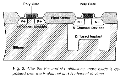
HP's bulk CMOS process uses local oxidation of silicon to attain a more planar topology that lends itself to easy metal coverage and to maximize device density. Without local oxidation another masking step would be required, and P + and N+ guard rings would also be needed to prevent parasitic leakage paths. The source and drain diffusions are partially separated by the field oxide, which provides an additional margin against adjacent diffusions punching through. Figs. 1, 2, 3, and 4 show the device cross-section after various processing steps.
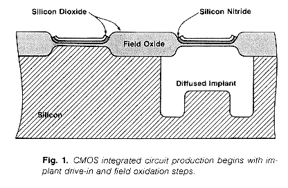
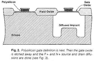
P-well doping (Fig. 1) is accomplished by using ion implantation techniques. This results in well-controlled characteristics of the N-channel devices. Self-aligned polysilicon gates (Fig. 2) are used to minimize the gate-to-source or gate-to-drain overlap capacitance, thus enhancing the performance of the MOS transistors. The polysilicon is heavily doped in the field region and serves as a layer of conducting interconnect in addition to the metal.
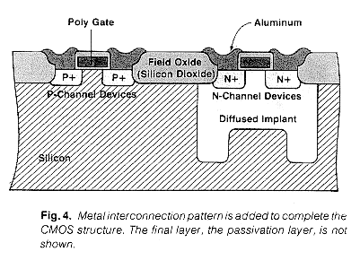
The intermediate oxides in this process are deposited using the low-pressure chemical vapor deposition (LPCVD) technique, which provides improved oxide integrity and excellent step coverage. The resultant oxides are also more dense, which helps in contact-mask oxide etching because denser oxides have a lower and more controllable etch rate than other forms of deposited oxides. Different oxide thicknesses over the various contacts make the contact-mask etch a critical step that needs and receives close scrutiny.
The passivation layer to protect the circuit on the chip is plasma-deposited silicon nitride, which results in a protective barrier impervious to humidity and ionic contamination. This was needed to ensure the long-term reliability of the ICs in a hybrid or plastic package.
The well-being of the entire process is monitored by probing five test chips on each wafer. These test chips yield valuable information about device parameters such as device threshold voltage, junction breakdown voltage, and junction and parasitic leakage currents, along with data on gate oxide and metal step coverage integrity, and so on. The test chip usually provides the first hint of a process malfunction and in a normal mode gives statistical information on the process for trend-charting. It is also sometimes used for verifying circuit design concepts.
Latch-up via parasitic PNPN transistors is a very common problem in all CMOS processes and special techniques have to be implemented in both circuit design and processing to minimize its impact. Fig. 5 shows the cross-section and equivalent circuit of these four-layer devices.
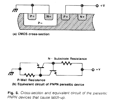
Normally the PNP transistor (formed by the P+ diffusion, the N- substrate, and the P well) and the NPN transistor (formed by the N- substrate, the P well, and the N+ diffusion) are biased off. When abnormally high currents are present in either the P well or the substrate, the emitter junctions can be forward-biased, thereby turning on the parasitic PNPN device.
Sensitivity to latch-up is reduced in two ways. The first is by increasing the spacing between the P+ and P-well junction to reduce the gain of the PNP transistors. The second is by ensuring that the P wells are adequately grounded.
The initial CMOS process development effort was started at ICL under the tutelage of John Moll and Juliana Manchu. Thanks also go to Bob Grimm and Pat Castro for nurturing the effort for over two years and then doing the initial pilot production. At Corvallis Division Dave Rupprecht and his team were responsible for the initial setup of the process in production. Kuldip Sethi and his team also contributed to the initial process characterization.
Norman L. Johnson
Born in Sioux Falls, South Dakota, Norm Johnson received his BSEE and MSEE degrees from the South Dakota School of Mines and Technology in 1966 and 1967 respectively. His PhD degree in electrical engineering is from Oregon State University (1974). With HP since 1977, he worked on several of the HP-41C CMOS integrated circuits, including the CPU and display driver. Before coming to HP he was a process development engineer working on MNOS, N-channel SOS, and N-channel silicon gate integrated circuits. Married with two sons and living in Corvallis, Norm and his family enjoy outdoor activities and camping in the beautiful Oregon countryside. He also does woodworking.
Vijay V. Marathe
A native of Hyderabad, India, Vijay Marathe received his B.Tech degree in electrical engineering from the Indian Institute of Technology, Bombay, in 1964. He earned his MSEE degree from the University of California at Berkeley in 1966, and the following year came to HP. Since then he has worked in nearly all of HP's IC operations, including those at Santa Clara, Cupertino, the Desktop Computer Division and the integrated circuit laboratory of HP Laboratories. He was responsible for setting up the CMOS operation at the Corvallis Division and is now working in the components operation there. Vijay also holds an MBA degree, received in 1976 from Santa Clara University, and a DEE degree from the same university (1973). He is named inventor on two patents related to the HP-01 Calculator/Watch project. A member of the American Management Association and a first generation emigrant to the United States, Vijay has spent the past few years researching the various religions of the world, a subject he finds fascinating. He's an avid tennis and ping pong player and has been a stamp collector for 25 years. He and his wife and two children make their home in Corvallis, Oregon.
![]() Go back to the HP Journal library
Go back to the HP Journal library
![]() Go back to the main exhibit hall
Go back to the main exhibit hall