![]() The Museum of HP Calculators
The Museum of HP Calculators
By Henry J. Kohoutek
THE PROCESSING UNIT for HP 9800-Series calculators is a microprogrammed 16-bit serial processor that is capable of executing 75 basic machine-language instructions. The processor
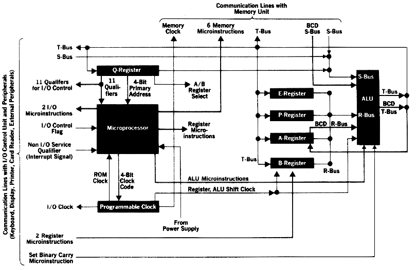
The processing unit is implemented with MSI bipolar logic circuitry with strong emphasis on read-only memories Central control of the processor, memory, and I/O unit is nested in microprograms stored in these ROMs in the microprocessor section of the processor (see Fig. 1). The microprocessor executes machine-language instructions in cycles by following these microprograms.
It's important to note that there are two levels of ROM in 9800-Series Calculators. Keystrokes or user program statements initiate sequences of machine-language instructions. These sequences are stored in MOS ROMs that are part of the memory system (see article, page 22). For each of the 75 machine-language instructions there is a sequence of microinstructions stored in the microprocessor's bipolar ROM. The ROM modules that plug into 9800-Series Calculators expand the higher-level MOS ROM, not the microprocessor ROM, which is the same in all models.
The microprocessor ROM, which holds the microprogrammed execution routines for individual machine-language instructions, consists of a block of seven bipolar read-only memories organized in 256 words of 28 bits. Fast routine execution times, based on an internal clock frequency of 8 MHz, help speed up all keyboard functions.
Fig. 1 is a block diagram of the 9800 processor, showing its organization and its relationships with the memory and input/output control unit. The processor has an R-S-T bus configuration. Two buses, R and S, carry data to the arithmetic/logic unit (ALU), and the third bus, T, carries the ALU output.
There are five principal working registers which communicate via the bus system and the ALU, under control of the microprocessor's instruction logic and the number of shift clock pulses that have occurred.
P-register is the calculator's program counter. By going through a step-by-step counting sequence, it causes successive instructions to be read out of the memory. The sequential stepping can be altered by execution of skip or jump instructions, thus causing the program to continue at a different memory address. During execution of some instructions, the P-register contains a special binary word that is used to simplify digit and word counting.
A-register is one of the calculator's two accumulators. It is capable of accepting results of both binary and decimal arithmetic operations. When a decimal operation is performed, the four-bit result is temporarily received in bits A3-A0 of the A register.
B-register is another accumulator. It has the same capabilities as the A-register except for decimal arithmetic.
E-register represents a flexible four-bit extension of all other registers. It's used for left and right shifts with binary-coded-decimal data occupying several memory locations.
Q-register contains the program instruction currently being executed. Its individual bits can be tested as qualifiers to perform microprogram branching according to the instruction code. In the final part of microprogram routines when the instruction code has been fully recognized, the Q-register is used for temporary storage of internal processor information.
The programmable clock contains the system clock generator, along with logic which, by decoding the clock field of the microinstruction, causes the correct number of shift pulses to be issued to the working registers and the ALU. This scheme makes it possible to have variable cycle time for each state of the microprogram, and results in a substantial saving in microprocessor ROM. A ROM clock pulse occurs once for each microprogram state and is applied to the ROM address flip-flops.
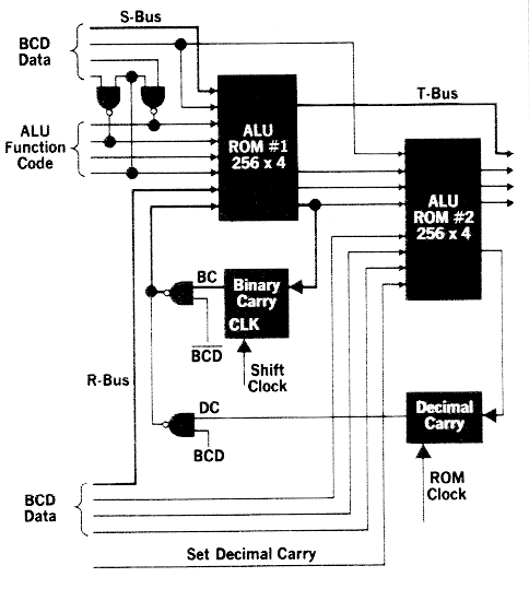
The binary/BCD arithmetic logic unit (ALU) performs one-bit binary logic and arithmetic operations, as well as four-bit binary-coded-decimal arithmetic operations. Coded results for all logic and arithmetic operations are nested in a form of special look-up table on two bipolar 1024-bit ROM's. Data from working registers and the carry flip-flop, together with the microinstruction to be executed serve as ALU inputs. These inputs define a unique ROM address where the proper result is encoded, and gates are enabled to place this result on the ALU output lines. The states of two ALU carry flip-flops are communicated to the microprocessor where they are recognized as special qualifiers. The ALU organization is shown in Fig. 2.
The processor communicates with the memory unit and the I/O control unit via the T-bus and the S-bus and by special groups of memory and I/O microinstructions. The processor's clock circuitry synchronizes all units by generating memory clock pulses and I/O clock pulses.
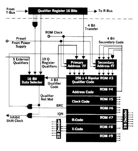
Detailed structure of the microprocessor is shown in Fig. 3.
The primary and secondary address flip-flops form a microprogram counter, which selects the memory location where the microinstruction to be executed is stored. Each microinstruction is 28 bits wide and contains information to control the data flow in the system by enabling appropriate gates and generating the proper number of shift clock pulses.
Also included is information to define the ROM address of the next microinstruction. Thus instead of being limited to a fixed address sequence, the microprogram may in effect execute almost a random walk through the ROM addresses.
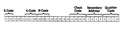
The microinstruction format is shown in Fig. 4. The four-bit qualifier code in each microinstruction serves a dual purpose. If branching is desired, the microinstruction BRC must be programmed. If the preceding microinstruction is BRC, the four-bit qualifier code selects the proper qualifier to be tested and the primary address of the next micro-instruction is the same as the current one. If the preceding microinstruction is not BRC the qualifier code defines the primary address of the next micro-instruction.
A single-chip 16-bit data selector permits any one of the 16 qualifiers to be tested according to the qualifier code. If branching is to occur, the micro-instruction BRC, along with a signal from the data selector, defines the least significant bit of the secondary address of the next microinstruction, according to the result of the qualifier test.
A special microinstruction, IQN, inhibits all shift clock pulses from the clock decoder in case the selected qualifier condition was not met. This in effect prevents execution of microinstructions in that ROM state.
To minimize the microinstruction width the operation codes for clock decoder, ALU, bus-gate control, and so on, are coded into groups and decoded by hardware into individual signals.
Besides the 75 basic machine-language instructions, the system can also perform indirect memory calls, interrupts, I/O calls, and a simple resident diagnostic of its own performance in start-up conditions.
The microinstructions that control the calculator's processor and memory define the lowest language that can control the machine hardware. Therefore, for testing 9800 Series Calculators on the production line and in the field, a tester was designed to execute machine diagnostics on the microprocessor level, following a "start-small" strategy.
The tester organization is very similar to that of the microprocessor, but instead of machine-language execution routines, a system of tests is nested in a group of ROM's. Virtually identical organization, hardware, and timing of microprocessor and tester assures similarity between working and testing conditions from a physical and an electrical point of view. This means that the diagnostic information represents a realistic picture of the state of the tested machine.
The tester hardware also contains logic for convenient manual operations, simple aids for trouble-shooting in case an error is detected, and circuitry for computer interface.
Test routines are organized in a sequence There is a pretest, a series of 22 tests, and a posttest to check magnetic-card-reader mechanics. The pretest is a manually controlled resident microdiagnostic routine designed to test the tester's hardware. The start-small strategy is reflected in the test sequence, which begins with very simple tests of binary logic functions of the ALU, and continues through register tests to complex tests of the entire ALU and memory. Each test uses only successfully tested parts of the machine hardware and evaluates only a small new part of the hardware. This makes it easy to locate failures when an error is discovered.
![]() Go back to the HP Journal library
Go back to the HP Journal library
![]() Go back to the main exhibit hall
Go back to the main exhibit hall