The calculator used a 16-bit HP processor implemented on three NMOS chips. The three chips were the:
These three chips were packaged in a small hybrid circuit with several buffer chips. Registers on the processor chips were memory mapped allowing communications between the chips through a 32-word window in memory.
Memory was word-addressed and therefor required only 15 bits to address 64K bytes. That left the most significant bit in each address free to indicate indirect addressing. If the bit was a one, the word at the address was treated as another address (and fetched).
All communication from the CPU to all read/write and read-only memory was by means of a 16-line bus with time multiplexed data, addresses and instructions. The maximum addressable memory was 64K bytes and the memory cycle time was 880 nanoseconds.
The 24K bytes of operating system ROM were mounted in a long plug-in module that slid in at the lower right side of the calculator. This allowed independent testing of the ROM and made field ROM upgrades a simple affair.
Additional ROMS containing optional language features could be plugged into four slots below the keyboard. All ROMs were composed of HP-developed 16K bit NMOS chips.
The calculator used 4K bit RAM chips. 8K bytes of RAM was standard with expansion to 32K possible. However, full expansion of RAM precluded the use of some ROMS due to lack of address space. This probably explains why HP 9825s seem to be found most commonly in the 24K byte RAM configuration.
Originally, the HP 9825 came with a low-profile snap feel keyboard like that of the HP 9815A/S. This keyboard saved space and money compared to the earlier designs. HP later reverted to the older keyboard designs for unknown reasons. (Perhaps it was simply because that was how most people expected a QWERTY keyboard to look and feel.)
The HP 9825 design team had goals for lighter weight and tighter tolerances the earlier models. This led them to abandon the earlier sheet metal and go to a hard structural foam which allowed the modern curved exterior and accommodated attachment points to be molded where needed inside. This case was metalized on the inside and grounded for RF protection.
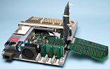
Circuit boards were mounted horizontally using a special stacked/hinge design. This allowed one or more boards to be folded up and away for easy access. (The calculator could be turned on and running when all this folding took place which made diagnostics easier.) The hinges came apart without tools when a board needed to be removed.

|
Picture of interior of HP 9825. This picture shows several boards flipped up. Since the bus was flexible, the machine could run in this state. |